
The N-Type Solar Cell
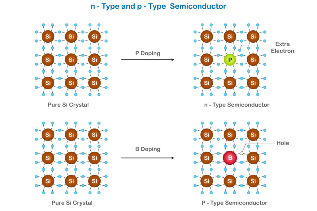
For years, most solar modules were built using P-type silicon wafers. They still dominate older residential systems today. But the industry is rapidly shifting toward N-type technology because it solves several physical limitations built into traditional P-type cells.
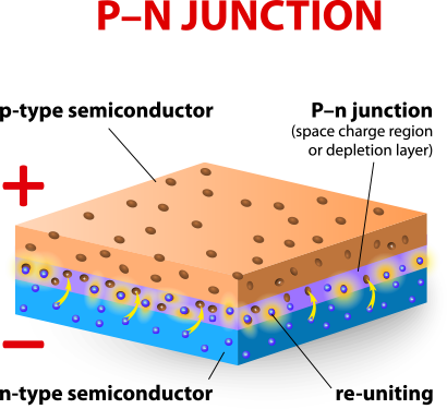
Both P-type and N-type cells still use a PN junction. Every silicon solar cell needs one. The difference is the starting wafer material.
A traditional P-type cell begins with a boron-doped silicon wafer. Manufacturers then diffuse phosphorus into one side of the cell to create a thin N-type layer and form the PN junction.
N-type cells reverse the structure. The wafer itself is phosphorus-doped, while a thin boron-doped layer creates the opposite side of the junction.
That sounds like a small change, but it fixes one of the biggest weaknesses in older solar technology.
P-type wafers are vulnerable to boron-oxygen defects. Under sunlight, those defects create recombination centers that steal electrons before they can become usable electricity. This is one reason older P-type modules experience higher light-induced degradation.
N-type wafers avoid most of that problem entirely.
The reason this matters is because the PN junction only separates charge carriers. After electrons and holes are separated, they still need to travel through the silicon itself to reach the electrical contacts. The wafer is not just structural material. It is the transport medium.
Electrons also move through silicon more easily than holes do. In N-type material, electrons become the majority carriers, giving the cell a built-in physics advantage.
That means modern N-type modules often provide:
- lower degradation rates
- better high-temperature performance
- longer carrier lifetimes
- better low-light production
- higher bifacial performance
- higher long-term energy yield
Some modern N-type modules are now degrading at rates as low as 0.25% per year. Many older modules were closer to 0.5% or higher.
That difference compounds over decades.
The industry’s biggest current N-type architecture is TOPCon, short for Tunnel Oxide Passivated Contact.
TOPCon cells use an ultra-thin oxide layer measured in nanometers. It is thin enough that electrons can quantum tunnel through it while recombination losses are reduced. Manufacturers are essentially engineering electron flow at the atomic scale now.
Modern TOPCon modules are regularly reaching 22-24% module efficiency in production products.
Another major architecture is HJT, or Heterojunction Technology.
HJT combines crystalline silicon with ultra-thin amorphous silicon layers. These cells often perform especially well in heat because their temperature coefficients are excellent. On hot roofs, that can matter more than people realize.
Temperature is one of the biggest hidden enemies of solar performance.
A module rated at 440 W under Standard Test Conditions is tested at:
- 1000 W/m² irradiance
- 25°C cell temperature
- perfectly controlled lab conditions
Real roofs get much hotter than that.
On a sunny summer day, cell temperatures can exceed 60°C. Even while sunlight is strong, voltage drops as temperatures rise.
That is why efficiency improvements matter so much. Engineers are constantly fighting recombination losses, thermal losses, resistive losses, and optical losses all at once.
Modern cells are also getting thinner while becoming more efficient. Manufacturers are learning how to control photons and electron behavior more precisely instead of simply using more silicon.
And despite how advanced solar has become, the core mechanism is still surprisingly elegant:
Photons strike silicon.
Electrons get excited into the conduction band.
The PN junction separates charge.
The wafer transports carriers.
Metal contacts collect current.
That entire process happens billions of times per second inside every module on the roof.